Get Grounded: What You Need to Know About ESD and RF Devices (Part 1 of 3)

July 26, 2018

esd-rollup1_320x180.jpgThis is the first blog in a three-part series looking at ESD protection in mobile handsets.

The electrostatic discharge (ESD) phenomenon has been around since the beginning of time. Our first experience with ESD most often comes in childhood when you touch a metal doorknob on a dry wintry day. Zap, you get a shock — courtesy of electrostatic discharge. This momentary discomfort usually isn’t problematic for humans, but sensitive electrical circuits can be destroyed by even a small amount of ESD.  

Mobile designers continue to face challenges of when and how to address this natural phenomenon. This blog explains why system-level ESD protection matters, providing insight on test models and strategies to improve system-level ESD protection in mobile devices.
 

Testing for ESD models and waveforms

The human body and its clothing can store between 500 V and 2,500 V of electrostatic charge during a day, but a human can only feel ESD pulses that are between 3,000 and 4,000 V. This is far above the level that damages electronic circuits, even if a human can’t detect it.

Designers must address ESD at many points — at the component manufacturers, during their design phases and at the end of their design work. In short, ESD protection requires a multifaceted approach.

Typically, integrated circuit (IC) manufacturers design, test and qualify their ICs according to ESD industry standards. This protects against physical damage during IC production or assembly onto PC boards. The two tests that are typically used for ESD include the following:

  • Human Body Model (HBM). This test simulates an ESD event in which a human body discharges the accumulated electrostatic charge by touching an IC. It’s modeled by a charged 100 pF capacitor and a 1.5 kΩ discharging resistor.
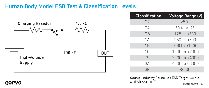
Human Body Model (HBM) ESD Test & Classification Levels

  • Charged Device Model (CDM). This test simulates charging and discharging events that occur in production equipment and processes. The device acquires a charge through some frictional processes or electrostatic induction process and then abruptly touches a grounded object or surface.
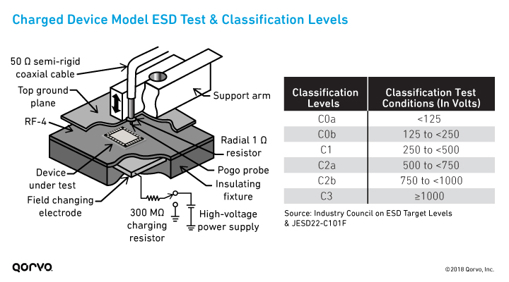
Charged Device Model (CDM) ESD Test & Classification Levels

While device-level testing helps provide a measure of ESD robustness for the IC, system-level testing measures the protection of the electronic devices when in the field (i.e., in the original equipment manufacturer [OEM] device or end product).

To best understand the ESD protection required for a final product, the OEM should design using a system-level ESD approach and then test the final product according to the International Electrotechnical Commission (IEC) ESD standard 61000-4-2. IEC 61000-4-2 is recognized as the industry standard for end-product ESD testing and rating. This test determines the vulnerability of the system to external ESD events in the field.

The following figure compares the amount of energy and peak current in three kinds of pulses:

  • System-level IEC 61000-4-2
  • Device-level HBM
  • Device-level CDM

The IEC ESD event pulse is noticeably stronger, and thus is more difficult for a device in a system to pass. Although device-level testing (HBM and CDM) is helpful and provides a baseline for ESD robustness, it doesn't always determine survivability during a system-level IEC test.
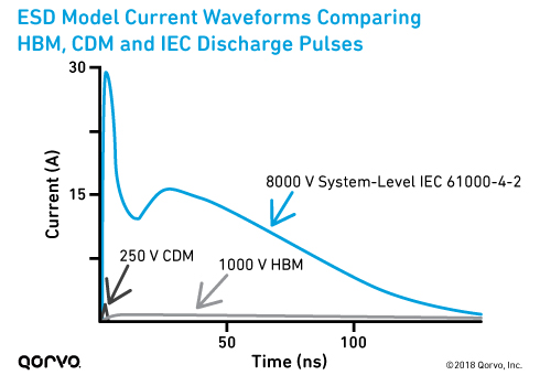
ESD Model Current Waveforms Comparing HBM, CDM and IEC Discharge Pulses

To display this concept further, the following table shows the differences between component testing and system-level IEC testing. As you can see, there’s a big difference — the system stress levels are higher. The takeaway: The system design must meet more stringent requirements than device-level designs.
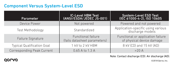
Component-Level Versus System-Level IEC ESD Testing


The problem with inadequate testing

Performing system-level ESD tests during the development process can be problematic. For example, testing ESD on evaluation/incomplete board assemblies doesn't provide a full picture. Results on these assemblies don't guarantee the final result in the completed system.

Device-level ESD tests (i.e., HBM and CDM) were designed to generate repeatable and reproducible results for discrete components in a factory with the appropriate ESD controls. This is known as an ESD protected area (EPA). However, these tests aren’t intended to address the full range of real-world product-level ESD events outside of the EPA.
 

The key to product robustness: System-level ESD

Instead, the key to an ESD-robust system design is to consider the effects of ESD in the system. To obtain a system-level perspective, it’s paramount that designers understand and address the following:

  • The system-level stress event and its effect on the entire product. Device-level ESD test results provide minimal information for a system ESD design, because they can't reflect what the electronic device experiences during the IEC ESD event.
  • The board-level interactions in the system, along with the transient behavior of the pins that contact the outside of the electronic part during ESD stress.
  • Efficient characterization methods like component-level transmission line pulse (TLP) data, to analyze the IC, board and system interactions.

System-level ESD protection strategies depend on physical design, product requirements and product cost.

Go in Depth
Learn more about system-level ESD:

  • System Level ESD: Part 1, Common Misconceptions and Recommended Basic Approaches (Industry Council on ESD)

The best approach: System-efficient ESD design (SEED)

System-efficient ESD design (SEED) is a system-level approach that considers the transient responses of all components in the system. SEED methodology also includes the physical effect of an IEC stress applied at the external port of the PC board on the IC pin. 

SEED is a co-design methodology that realizes both on-board and on-chip ESD protection. Using SEED, you analyze and achieve system-level ESD robustness. The approach requires a full understanding of interactions between external ESD pulses, full system-level board design, and device pin characteristics during an ESD stress event.

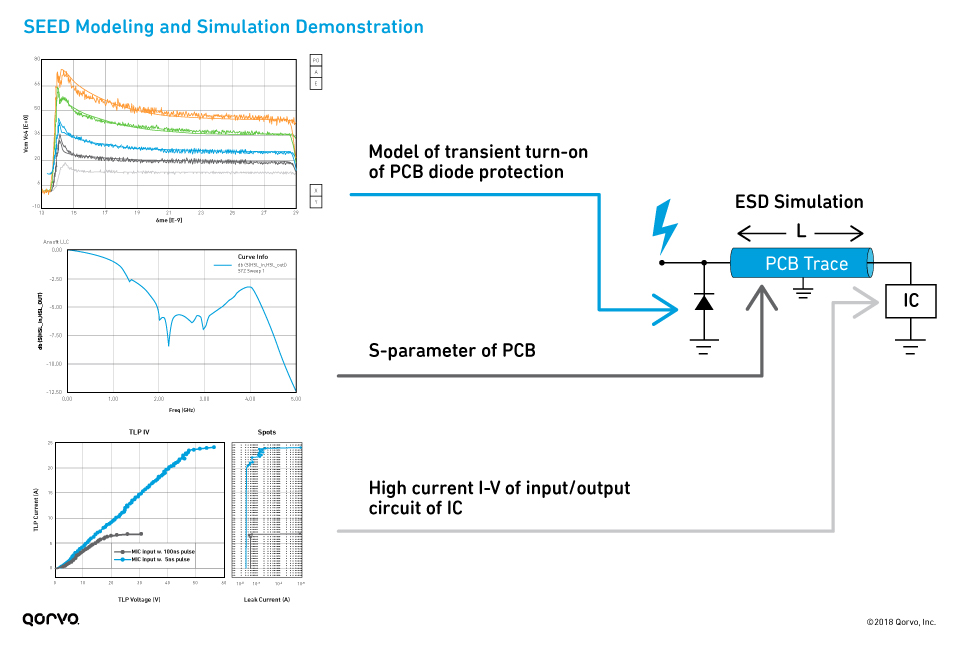
SEED methodology is the best approach for systematic and robust system-level ESD protection. As shown in the next figure, SEED uses the following to design system-level ESD protection:

  • Quasi-static TLP current-voltage (I-V) curve data
  • Transient simulations
  • S-parameter PC board data
  • IC I-V circuit measurements 

Demonstration of SEED Design and Simulation

We'll go into the details of SEED in Part 2 and Part 3 of this blog series. But as a general introduction to SEED:

  • The PC board’s ESD protection forms the primary protection, preventing physical damage to the IC or system.
  • The on-chip protection serves a secondary protection role.

 
The fundamental concept of SEED is to limit the damaging ESD pulses from reaching the internal IC pins. Proper system-level ESD design is achieved by performing and analyzing an ESD system-level simulation.
 

Next up: ESD protection strategies for RF front-end designs

It’s no secret that it’s important to approach ESD strategically in your mobile designs. Doing so reduces design engineering cycle times, ESD failure and R&D expenses.

In the next post in this three-part blog series, we dig further into ESD protection components and different strategies to mitigate the effects of ESD on your mobile RF designs. Part 3 will explain how to use SEED methodology, simulation and modeling to determine your system-level ESD protection.
 

Read all the blogs in our series about overcoming ESD challenges in mobile devices:

  • Part 1: Get Grounded: What You Need to Know About ESD and RF Devices (this post)
  • Part 2: ESD Design Strategy for Mobile Devices: Your Tools for SEED
  • Part 3: SEED Methodology for Optimizing an ESD RF Front-End Design

Get Grounded on ESD

Stay up to date with us.

Sign up for notification on new products, product/process change notifications (PCNs) and end of life (EOL) alerts.

Sign Up

Qorvo products are at work connecting, protecting and powering the planet. We bring core radio frequency (RF) and power technologies and solutions to automotive, consumer, defense & aerospace, industrial & enterprise, infrastructure and mobile markets.

Stay Connected

  • Facebook
  • X
  • LinkedIn
  • YouTube
  • Products
  • Solutions
  • Design Hub
  • New Products
  • Product Compliance
  • Blog Posts
  • Events & Trade Shows
  • News Releases
  • Success Stories
  • Technical Articles
  • About Us
  • Careers
  • Corporate Videos
  • Quality
  • Locations
  • Investors
  • How to Buy
  • Forums
  • Portals
  • Contact Us
  • Subscription Center
Site MapFeedbackLegalPrivacySupply Chain Transparency

© 2026 Qorvo US, Inc

|

+1-833-641-3810

Get Grounded: What You Need to Know About ESD and RF Devices (Part 1 of 3)

July 26, 2018

esd-rollup1_320x180.jpgThis is the first blog in a three-part series looking at ESD protection in mobile handsets.

The electrostatic discharge (ESD) phenomenon has been around since the beginning of time. Our first experience with ESD most often comes in childhood when you touch a metal doorknob on a dry wintry day. Zap, you get a shock — courtesy of electrostatic discharge. This momentary discomfort usually isn’t problematic for humans, but sensitive electrical circuits can be destroyed by even a small amount of ESD.  

Mobile designers continue to face challenges of when and how to address this natural phenomenon. This blog explains why system-level ESD protection matters, providing insight on test models and strategies to improve system-level ESD protection in mobile devices.
 

Testing for ESD models and waveforms

The human body and its clothing can store between 500 V and 2,500 V of electrostatic charge during a day, but a human can only feel ESD pulses that are between 3,000 and 4,000 V. This is far above the level that damages electronic circuits, even if a human can’t detect it.

Designers must address ESD at many points — at the component manufacturers, during their design phases and at the end of their design work. In short, ESD protection requires a multifaceted approach.

Typically, integrated circuit (IC) manufacturers design, test and qualify their ICs according to ESD industry standards. This protects against physical damage during IC production or assembly onto PC boards. The two tests that are typically used for ESD include the following:

  • Human Body Model (HBM). This test simulates an ESD event in which a human body discharges the accumulated electrostatic charge by touching an IC. It’s modeled by a charged 100 pF capacitor and a 1.5 kΩ discharging resistor.

Human Body Model (HBM) ESD Test & Classification Levels

  • Charged Device Model (CDM). This test simulates charging and discharging events that occur in production equipment and processes. The device acquires a charge through some frictional processes or electrostatic induction process and then abruptly touches a grounded object or surface.

Charged Device Model (CDM) ESD Test & Classification Levels

While device-level testing helps provide a measure of ESD robustness for the IC, system-level testing measures the protection of the electronic devices when in the field (i.e., in the original equipment manufacturer [OEM] device or end product).

To best understand the ESD protection required for a final product, the OEM should design using a system-level ESD approach and then test the final product according to the International Electrotechnical Commission (IEC) ESD standard 61000-4-2. IEC 61000-4-2 is recognized as the industry standard for end-product ESD testing and rating. This test determines the vulnerability of the system to external ESD events in the field.

The following figure compares the amount of energy and peak current in three kinds of pulses:

  • System-level IEC 61000-4-2
  • Device-level HBM
  • Device-level CDM

The IEC ESD event pulse is noticeably stronger, and thus is more difficult for a device in a system to pass. Although device-level testing (HBM and CDM) is helpful and provides a baseline for ESD robustness, it doesn't always determine survivability during a system-level IEC test.

ESD Model Current Waveforms Comparing HBM, CDM and IEC Discharge Pulses

To display this concept further, the following table shows the differences between component testing and system-level IEC testing. As you can see, there’s a big difference — the system stress levels are higher. The takeaway: The system design must meet more stringent requirements than device-level designs.

Component-Level Versus System-Level IEC ESD Testing


The problem with inadequate testing

Performing system-level ESD tests during the development process can be problematic. For example, testing ESD on evaluation/incomplete board assemblies doesn't provide a full picture. Results on these assemblies don't guarantee the final result in the completed system.

Device-level ESD tests (i.e., HBM and CDM) were designed to generate repeatable and reproducible results for discrete components in a factory with the appropriate ESD controls. This is known as an ESD protected area (EPA). However, these tests aren’t intended to address the full range of real-world product-level ESD events outside of the EPA.
 

The key to product robustness: System-level ESD

Instead, the key to an ESD-robust system design is to consider the effects of ESD in the system. To obtain a system-level perspective, it’s paramount that designers understand and address the following:

  • The system-level stress event and its effect on the entire product. Device-level ESD test results provide minimal information for a system ESD design, because they can't reflect what the electronic device experiences during the IEC ESD event.
  • The board-level interactions in the system, along with the transient behavior of the pins that contact the outside of the electronic part during ESD stress.
  • Efficient characterization methods like component-level transmission line pulse (TLP) data, to analyze the IC, board and system interactions.

System-level ESD protection strategies depend on physical design, product requirements and product cost.

Go in Depth
Learn more about system-level ESD:

  • System Level ESD: Part 1, Common Misconceptions and Recommended Basic Approaches (Industry Council on ESD)

The best approach: System-efficient ESD design (SEED)

System-efficient ESD design (SEED) is a system-level approach that considers the transient responses of all components in the system. SEED methodology also includes the physical effect of an IEC stress applied at the external port of the PC board on the IC pin. 

SEED is a co-design methodology that realizes both on-board and on-chip ESD protection. Using SEED, you analyze and achieve system-level ESD robustness. The approach requires a full understanding of interactions between external ESD pulses, full system-level board design, and device pin characteristics during an ESD stress event.

SEED methodology is the best approach for systematic and robust system-level ESD protection. As shown in the next figure, SEED uses the following to design system-level ESD protection:

  • Quasi-static TLP current-voltage (I-V) curve data
  • Transient simulations
  • S-parameter PC board data
  • IC I-V circuit measurements 

Demonstration of SEED Design and Simulation

We'll go into the details of SEED in Part 2 and Part 3 of this blog series. But as a general introduction to SEED:

  • The PC board’s ESD protection forms the primary protection, preventing physical damage to the IC or system.
  • The on-chip protection serves a secondary protection role.

 
The fundamental concept of SEED is to limit the damaging ESD pulses from reaching the internal IC pins. Proper system-level ESD design is achieved by performing and analyzing an ESD system-level simulation.
 

Next up: ESD protection strategies for RF front-end designs

It’s no secret that it’s important to approach ESD strategically in your mobile designs. Doing so reduces design engineering cycle times, ESD failure and R&D expenses.

In the next post in this three-part blog series, we dig further into ESD protection components and different strategies to mitigate the effects of ESD on your mobile RF designs. Part 3 will explain how to use SEED methodology, simulation and modeling to determine your system-level ESD protection.
 

Read all the blogs in our series about overcoming ESD challenges in mobile devices:

  • Part 1: Get Grounded: What You Need to Know About ESD and RF Devices (this post)
  • Part 2: ESD Design Strategy for Mobile Devices: Your Tools for SEED
  • Part 3: SEED Methodology for Optimizing an ESD RF Front-End Design
Get Grounded on ESD

Stay up to date with us.

Sign up for notification on new products, product/process change notifications (PCNs) and end of life (EOL) alerts.

Sign Up

Qorvo products are at work connecting, protecting and powering the planet. We bring core radio frequency (RF) and power technologies and solutions to automotive, consumer, defense & aerospace, industrial & enterprise, infrastructure and mobile markets.

Stay Connected

  • Facebook
  • X
  • LinkedIn
  • YouTube
  • Products
  • Solutions
  • Design Hub
  • New Products
  • Product Compliance
  • Blog Posts
  • Events & Trade Shows
  • News Releases
  • Success Stories
  • Technical Articles
  • About Us
  • Careers
  • Corporate Videos
  • Quality
  • Locations
  • Investors
  • How to Buy
  • Forums
  • Portals
  • Contact Us
  • Subscription Center
Site MapFeedbackLegalPrivacySupply Chain Transparency

© 2026 Qorvo US, Inc

|

+1-833-641-3810

Qorvo
  • Products
  • Solutions
  • Design Hub
  • Support
  • About Us
Qorvo
Qorvo
Qorvo
  • Products
  • Solutions
  • Design Hub
  • Support
  • About Us
Qorvo
Qorvo