SEED Methodology for Optimizing an ESD RF Front-End Design (Part 3 of 3)
This is the last blog in a three-part series explaining various aspects of electrostatic discharge (ESD) and ESD system design for mobile devices.
- Part 1 introduced the basic concepts of ESD and its relation to system design.
- Part 2 provided strategic guidance to ESD system design, introducing the tools and components used for on-board ESD protection.
- Part 3 (this post) explains system-efficient ESD design (SEED) modeling techniques and considerations for the RF front-end (RFFE) design.
Putting it all together
Typically, system designers add ESD protection using a trial-and-error approach. The downside? It isn’t sufficient to address robust system design using only component-level ESD specifications. The goal is to predict the ESD performance of the final handset design to create a foolproof, one-pass system design with ESD protection incorporated.
One of the best approaches is to use models to simulate the IEC 61000-4-2 contact discharge pulses, so that you can determine your ESD performance before spending time and money on actual design prototypes.
To do this, we use the system-efficient ESD design (SEED) approach. If you're interested in the details of SEED, you can read more in this Industry Council for ESD white paper, System Level ESD Part I: Common Misconceptions and Recommended Basic Approaches.
SEED is a co-design methodology of on-board and on-chip ESD protection that helps analyze and achieve system-level ESD robustness. This approach requires a thorough understanding of the interactions between the external ESD pulses, full system-level board design, and device pin characteristics during an ESD stress event.
High-level steps to model and simulate for SEED
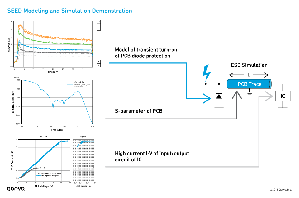
SEED methodology requires modeling and simulating the various components and traces of the system. At a high level, the steps to model and simulate using SEED methodology include the following:
Step 1: Gather information on the system, such as:
- PC board Gerber files, including PC board material specifications (stack-up file, transmission line specs, etc.)
- Transient voltage suppressor (TVS), inductor and capacitor device models (S‑parameters, I-V characteristics, ESD ratings, IV-TLP characteristics, etc.)
- RF front-end module I/O pin on-chip ESD protection models (IV-TLP measurements, S‑parameters, ESD ratings, etc.)
Step 2: Run transient and RF simulations to model the behavior of the ESD protection devices during system-level ESD stress and normal operation.
Detailed steps: How to simulate for SEED
Let’s step through a simple example to show how to use SEED methodology to design your ESD protection.
To begin, you’ll need to determine the isolation impedance required in the system to ensure the peak ESD current and voltage reaching the IC pin is within the on-chip (secondary clamp) protection capabilities. This is done by creating a simulation using IEC stress models and transmission line pulse (TLP) data of on-board TVS components (primary clamping) and the IC interface pins (secondary clamp).
Ultimately, your goal is to verify what you need for ESD protection for the system. To do that, complete the following steps:
- Create your ESD pulse.
- Load the Gerber files.
- Load all the other components into your modeling software.
- Run the simulation to determine the IEC stress level at the RFFE pin.
- Figure out which components you need for on-board ESD protection.
- Add the components to the model.
- Rerun the simulation to verify that the added components worked.
- Once you pass the ESD test, lay out your final PC board.
Let’s break down each step.
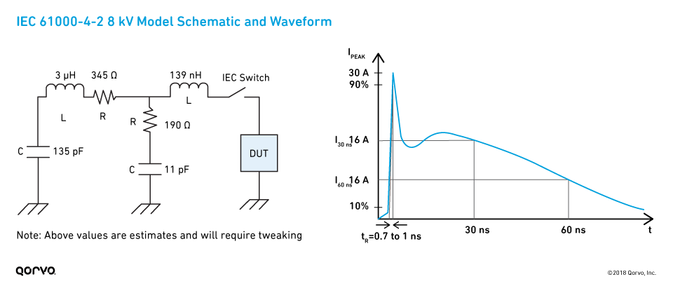
Step 1: Create the ESD pulse using IEC 61000-4-2 specification values
Load the model schematic of the RLC (resistor-inductor-capacitor) circuit as shown below into your simulation tool and verify that you get the waveform shown below. The model will simulate the ESD pulse. Note that some of the values may need tweaking to get that exact waveform.
Step 2: Load the Gerber files
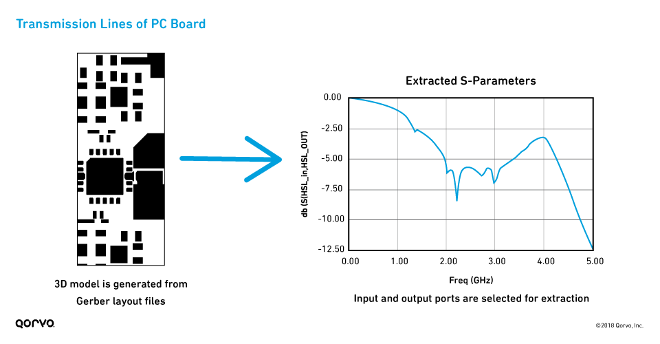
Next, use the 3D Gerber layout files to evaluate the PC board traces. Place these files in the modeling software. Model the layout traces, such as the dimensions of the microstrip lines.
Step 3: Load all the other components into your modeling software
These components include the following:
- TLP I/O device pin data
- Matching components
- Transmission line components
Step 4: Run your simulation
After you’ve loaded all the components, you want to see what your result is. At this point, you’re determining what your IEC stress level is at your RFFE pin. If that level exceeds the capabilities of the internal IC protection, then you’ll need to add on-board ESD protection, such as blocking caps, TVS diodes, etc.
Step 5: Figure out which components you need for on-board ESD protection
We covered different components and strategies for ESD protection in Part 2 of this blog series. Compare the individual protection components available to see what’s best to use for your design.
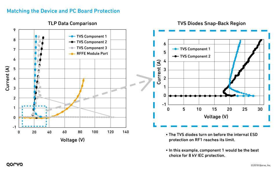
As an example, let’s say your simulation shows that your system needs additional on-board protection. The image below shows several components being reviewed by comparing data from TLP models. The orange line is the TLP model from an example Qorvo RFFE module port. The three other TLP models are the TVS components being evaluated. Based on the TLP data below, components 1 and 2 are the two best choices. They both meet our system requirements; however, when further analyzing the snap-back region, we chose component 1 because it triggers at a lower voltage. Triggering at a lower voltage means the TVS will be less likely to threaten our design by clipping our system signal performance.
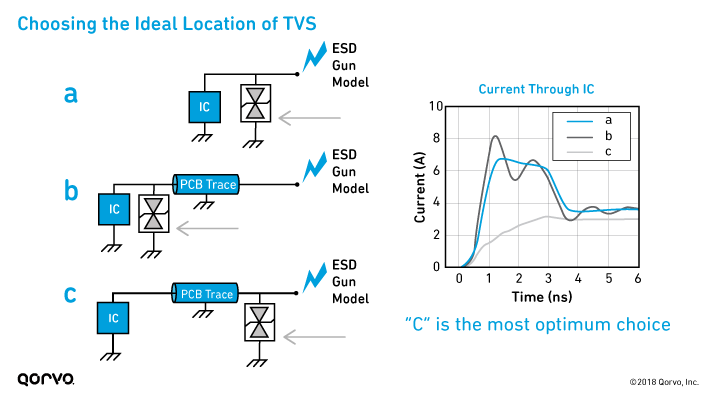
Once we’ve selected the TVS component, it’s important to place it in the correct on-board location. As you can see in the graph below, moving the TVS closer to the ESD entry point provides the most optimum decrease in ESD energy. The PC board trace can increase and decrease the first peak current amplitude depending on the TVS location.
Step 6: Add the components to the model
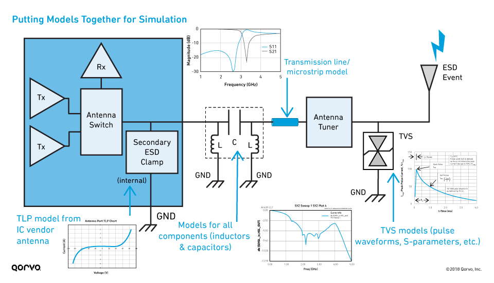
Once you’ve selected your ESD protection components (in our example, a TVS diode), you need to add them to the simulation, as shown below.
Step 7: Rerun the simulation to verify that the added on-board ESD components worked
Now that all the data is loaded into your simulation, you can run the transient simulations, analyze the current/voltage profiles along the RF path, and tune for minimum residual values on the internal pins (i.e., the module pins) as well as for system performance.
Note: Compact simulators can support transient simulations using S-parameter data. S-parameter data can also be converted to lumped models when required.
The ultimate goal is that your system design will pass IEC stress testing. Different applications will require different components or strategies, but modeling them early in your design phases will help increase the likelihood of passing IEC certification.
Step 8: Lay out the final PC board
Once your design passes the simulation, you can lay out your final system PC board. The difference with SEED is that you wait until after you’ve simulated and modeled the on-board ESD protection to lay out the system PC board — not early in the design phase.
Using SEED to increase your chances of passing ESD certification
SEED enables a better view into the system's performance and the capabilities of the IC ESD design. The IV-TLP curves provide the needed information about the on-chip, on-module and on-board ESD capabilities. When adding the transient simulations to the picture, you can evaluate the overall behavior of the on-chip and on-board ESD protection devices and how they perform together under system-level ESD stress. This allows you to build an optimal co-design with confidence from the initial stages of the hardware development — which ultimately increases efficiency and reduces overall design cost.
Read all the blogs in our series about overcoming ESD challenges in mobile devices:
- Part 1: Get Grounded: What You Need to Know About ESD and RF Devices
- Part 2: ESD Design Strategy for Mobile Devices: Your Tools for SEED
- Part 3: SEED Methodology for Optimizing an ESD RF Front-End Design (this post)